FPGA clock-enable divider
Choose an integer divider for a periodic enable pulse, inspect the frequency error, and generate a synchronous SystemVerilog counter.
Calculator
Divider calculation
The output enable rate is ftick = fclock / N. The calculator compares the floor and ceiling of the ideal ratio and chooses the divisor with the smaller absolute frequency error. Ties choose the smaller divisor. Counter width is max(1, ⌈log2N⌉), and the terminal count is N − 1.
Error in ppm = 106 × (factual − frequested) / frequested. Divisors from 1 to 4,294,967,295 are supported.
Using the generated module
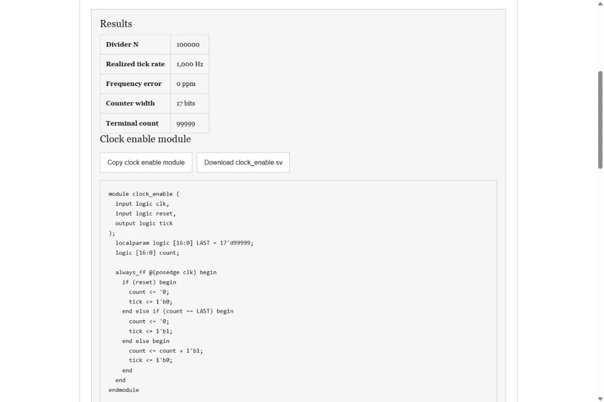
The reset is active-high and synchronous. After reset, the first tick occurs on the Nth rising edge. The registered tick remains high for one input-clock period when N > 1. For N = 1 it stays high after reset, enabling every cycle. Consume it inside logic clocked by the original clock, using if (tick).
A registered enable is observed by downstream sequential logic on the following rising edge. Account for that startup latency when aligning signals. Use dedicated AMD/Xilinx clocking resources such as an MMCM, PLL, or clock buffer when the design requires an actual routed clock domain.
Worked example
A 100 MHz input and 1 kHz enable rate give N = 100,000, a 17-bit counter, and terminal count 99,999, with zero frequency error.
Related tools
- SystemVerilog clock generator — Create simulation clocks for testing the generated enable counter.
- UART baud-rate divider — Include oversampling and serial-frame overhead in a UART calculation.
- Setup and hold timing budget — Check the register-to-register timing of logic driven by the input clock.